The Zeta-300 optical profilometer is a non-contact 3D surface topography measurement system with an integrated seismic isolation system and flexible configuration. This system uses ZDot ™ Technology and Multi Mode optical systems can measure various types of samples: transparent and opaque, low to high reflectivity, smooth to rough textures, and step heights ranging from nanometers to millimeters.
The configuration of Zeta-300 is flexible and easy to use, and it integrates six different optical measurement technologies. ZDot ™ The measurement mode can simultaneously capture high-resolution 3D data and True Color infinite focus images. Other 3D measurement techniques include white light interferometry, Nomarski interferometric contrast microscopy, and shear interferometry. ZDot or integrated broadband reflectometer can measure the thickness of thin films. Zeta-300 provides comprehensive measurements of step height, roughness, and film thickness, as well as defect detection capabilities, supporting research and production environments.

2、 Function
major function
Step height: 3D step height ranging from nanometers to millimeters
Texture: Smooth to very rough surface roughness and waviness
Appearance: 3D warping and shape
Stress: 2D thin film stress
Film thickness: 30nm to 100 μ m transparent film thickness
Defect detection: Capture defects larger than 1 μ m
Defect re inspection: Using KLARF files as navigation to measure the 3D surface morphology of defects or the location of cutting defects

FEATURES
Zeta-300 is a simple and easy-to-use optical profiler that uses ZDot and Multi Mode optical components, and has a wide range of applications:
A high-quality microscope that can be used for sample retesting or defect detection.
Z-Dot: Simultaneously collect high-resolution 3D data and True Color infinite focus images
ZXI: White light interferometry measurement technology, suitable for wide area measurement with high Z-axis resolution
ZIC: Interference contrast, suitable for surfaces with sub nanometer roughness and providing their 3D quantitative data
ZSI: Shear interferometry technology provides high-resolution images in the z-direction
ZFT: Measuring film thickness and reflectivity using an integrated broadband reflectometer
AOI: Automatic optical detection and quantification of defects on the sample
Production capacity: Fully automated measurement through sequencing and pattern recognition, supporting 3D scanning
Large size wafer measurement: The maximum measurement size can be expanded to 8 inches
Technical capabilities

3、 Application
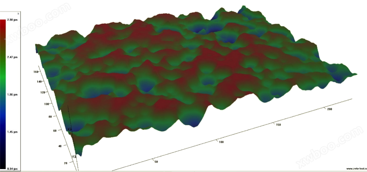
Schott Glass - Surface roughness
Can be used to test the morphology and surface roughness of transparent and opaque surfaces such as glass.

Solar cells - Measurement of surface morphology with different reflectivity
Easily obtain the surface morphology of complex differentiated reflectance samples.

MEMS devices - step height and roughness
The nanometer step accuracy of small-sized samples and the submicron step accuracy of large-sized samples.

Lens - Complete surface contour
The image stitching function can obtain the complete surface contour of large-area samples.

Polymer thin film - film thickness measurement
Can be used for thickness measurement of PI and PR films, and can generate film thickness mapping on the entire wafer.

Sapphire - patterned chip surface defects
Three dimensional contour scanning can be performed on specific defects and related measurements can be taken. Surface defects on the wafer can be distributed and mapped based on size, brightness, aspect ratio, etc.

4、 Other
Domestic users
Nanjing University
nanjing university of posts and telecommunications
Foreign users
mit
University of California, Dallas
Yale University
University of Texas at Austin
western digital
Application materials
bosch
University of Leicester
Seagate
Related literature
1. Maxym V.Rukosuyev, et al. One-step fabrication of superhydrophobic hierarchical structures by femtosecond laser ablation. Applied Surface Science. 2014,313,411-417.
2. H. N. Shubha, et al. Preparation of Self Assembled Sodium Oleate Monolayer on Mild Steel and Its Corrosion Inhibition Behavior in Saline water. ACS Appl. Mater. Interfaces. 2013,5,21,10738-10744.
3. Marta Palacios-Cuesta, et al. Fabrication of Functional Wrinkled Interfaces from Polymer Blends: Role of the Surface Functionality on the Bacterial Adhesion. Polymers. 2014, 6,11, 2845-2861.
4. Alberto Gallardo, et al. Chemical and Topographical Modification of Polycarbonate Surfaces through Diffusion/Photocuring Processes of Hydrogel Precursors Based on Vinylpyrrolidone. Langmuir. 2017,33 ,7, 1614-1622.
5. Aurora Nogales, et al. Wrinkling and Folding on Patched Elastic Surfaces: Modulation of the Chemistry and Pattern Size of Microwrinkled Surfaces. ACS Appl. Mater. Interfaces. 2017,9,23,20188-20195.
6. Olga Kraynis, et al. Suitability of Raman Spectroscopy for Assessing Anisotropic Strain in Thin Films of Doped Ceria. Adv. Funct. Mater. 2019, 1804433,2-7.

